Wednesday, November 23, 2011

Announcement: Update 14 for Altium Designer 10

The Altium Development team are pleased to announce the 14th update for Altium Designer 10.

This release focuses on further BugCrunch requests, with some of the notable enhancements including:

Variant support added to the STEP exporter

Now you can export mechanically accurate variants of the PCB assembly to 3rd Party Mechanical CAD tools. This will allow product enclosures and MCAD processes to be tuned to the specific needs of a design variant rather than having to accommodate all variants within a single MCAD model of the PCB design.

DXF/DWG added to Outjobs

With the addition of DXF/DWG export support in Outjobs, now you can automate the creation of this common output format and share settings across multiple projects.

Improved handling of duplicate pad names on a PCB component (footprint)

Some power devices have thermal pads that require connection to Ground (GND). Because these pads are often left out of the component’s schematic symbol, an explicit GND connection can not be made. Instead, PCB Component (footprint) creators sometimes force a GND connection by designating thermal pads with the same name as another GND pad on the PCB Component. This creates a 1:many relationship between schematic pins and PCB Component pads which Update 14 handles much better by ensuring that net connectivity is correctly established across all designated pads, regardless of whether they contain duplicated names.

Smoother cycling between designated routing layers

Altium Designer has long supported DRC rules to limit the layers that a net can be routed on. While these rules are checked and flagged as part of the DRC process, Altium Designer did not actively prevent illegal routes from being made during interactive routing. This latest update adds an additional layer of rule protection by ensuring that designers can only select layers permitted by the design rules during interactive routing; even if prohibited layers are also visible.

In total, 11 BugCrunch items have been included in this latest update, along with various other enhancements, with the full information listed in the release notes.

The delivery of this update affects the following 12 modules:

  1. System Components category: Altium Designer Base, PCB System, Schematic System, Soft Design Support
  2. Importers and Exporters category: Exporter - AutoCAD DWG, Exporter - DXF, Exporter - Hyperlynx, Importer - Allegro, Importer - PADS
  3. Output Generators category: Output - Gerber, Output - NC-Drill, Output - Gerber

This is the first release since the introduction of the patching system in Update 13. You should see a dramatic reduction in the size of the download required to install this update, and future ones, compared with previous updates. For example, the total download for Update 14 under the new system is 11MB, instead of 84MB which would have been experienced under the previous update system. Note though, the patching system works on your download cache so if you have cleared the cache since installing, it will require some modules (or all, depending on when you did it) to update using the previous update system, thus applying the full update to these modules.

Installation of the updated modules will bring their revision up to 10.771.23139. The Platform Build number will also update to 10.771.23139 as the Altium Designer Base module is updated.

To update your Altium Designer 10 installation, ensure you are using a license with valid subscription. Go to the Plug-in page (DXP >> Plug-ins and Updates) and select “Update All”. If you don’t see the update, use the “Refresh” link in top right hand corner of the Plugins page.

Note: If you are using a Private Server license or Standalone license, and you have renewed your subscription since activation, you will be required to reactivate your license to obtain this and future updates.

For those who installed directly from DVD, you can access the updates by changing a setting in preferences: System >> Installation Manager, change the Remote Repository Location to http://installation.altium.com

If you are wanting to install a new build containing this update, please download the latest Installer/Uninstaller to support this build.
 

Friday, November 18, 2011

Outsource your PCB work?

Have you considered outsourcing your PCB design work to a freelancer such as freelancer.com? Why not lighten your work load.

There are hundreds of thousands of satisfied customers from all over the world. That connect 2,959,683employers and freelancers globally from over 234 countries & regions

Thursday, November 10, 2011

Announcement: Update 13 now available for Altium Designer 10

The Altium Development team are pleased to announce the 13th update for Altium Designer.

This release is an important milestone in that it improves the update process through a new patching system, allowing us to deliver regular, frequent and significant updates in the future.

This new patching system has the benefit of delivering much smaller sized updates. Each patch is dramatically smaller than the files that are currently used in the update process, and the downloads required for an update are significantly reduced. It also provides more flexibility in the development that we can deliver, especially where a new feature or fix may require updates to all plug-ins. So once you have this update installed, future updates will be much smaller. Should you wish to use the patching with this update and take advantage of the smaller update now, please read instructions.

We have also included other enhancements to AD10, which we believe many of you will appreciate:

  1. A new Schematic CTRL+drag mode for accurately placing graphical objects without being constrained by the current grid settings
  1. Improvements to text rendering in the Schematic editor to provide better conformity between printed outputs and on-screen display
  2. Added option in the Find Similar Objects dialog to update the Inspector to the same scope
  3. Improvements have been made to the IDF Exporter.

Most of these, plus others, have resulted from requests submitted to BugCrunch. Thank you to those who submitted and voted for them.

For full information on this update, read the release notes.

The delivery of this update affects the following 10 modules:

  1. System Components category: Altium Designer Base, Altium Designer Support, PCB System, PCB Support, Schematic System, Soft Design Support
  2. Hardware Support Packages category: Device Support - Altera Stratix III
  3. Importers and Exporters category: Exporter - IDF, Importer - IDF
  4. Output Generators category: Output - ODB

Installation of these updated modules will bring their revision up to 10.747.23074. The Platform Build number will also update to 10.747.23074 as the Altium Designer Base module is updated.

To update your Altium Designer 10 installation, ensure you are using a license with valid subscription. Go to the Plug-in page (DXP >> Plug-ins and Updates) and select “Update All”. If you don’t see the update, use the “Refresh” link in top right hand corner of the Plugins page.

Note: If you are using a Private Server license or Standalone license, and you have renewed your subscription since activation, you will be required to reactivate your license to obtain this and future updates.

For those who installed directly from DVD, you can access the updates by changing a setting in preferences: System >> Installation Manager, change the Remote Repository Location to http://installation.altium.com

If you are wanting to install a new build containing this update, please download the latest Installer/Uninstaller to support this build.
 

Tuesday, October 18, 2011

New Product Release - Stackup Planner for Altium Designer

We are delighted to annouce the release of a product that finally allows you route to impedence in Altium Designer.

The Stackup Planner for Altium Designer imports the substrate configuration from the ICD Stackup Planner and automatically creates the corresponding Layers in Altium Designer, configuring the Layer Stackup Manager. Also, Design Rules for Trace Width, Clearance and Differential Pairs are automatically created enabling the user to route each layer and differential pair to the calculated single ended or differential impedance.

The interface also exports the Altium Designer Layers, from the Layer Stack Manager and Trace Width/Clearances into the ICD Stackup Planner for the calculation of impedance and trace current. The stackup can then be modified to obtain the desired impedances and imported back into Altium Designer.

The product includes both the ICD Stackup Planner and the Altium interface.

For more information or to request the demo, click here. <http://www.desktop-eda.com.au/products/StackupPlanner.html>

The Stackup Planner for Altium Designer is jointly developed by Desktop EDA and In-Circuit Design.

Monday, October 17, 2011

Custom Pad Shapes - soon to enter Beta

Over the past couple of months there has been development work underway to implement support for custom pads shapes, and this new enhancement is now approaching the stage of being ready to deploy to the Beta group.

Before this happens though, I would like to share the current state of development with you and gather any final thoughts, ideas and suggestions as feedback.

In my initial blog on custom pad shapes I detailed the three options available to tackle this issue: either original primitives could be enhanced and used to define the custom shape of a pad (along with net propagation through copper and mask generation); the pad object could itself be enhanced with new capabilities; or finally, a new ‘custom shaped pad’ object could be added.

The feedback you provided in response to the blog was seminal in helping me understand your perspective and design this new feature.

The result is that three new enhancements have been added to support the generation and management of custom pads in Altium Designer:

1. General primitives can generate solder and paste mask expansions.

Any track, arc, fill or region on the top or bottom layer are now able to generate solder and paste masks. In a similar way to how the masks are generated for pads, the masks for these objects can be manually specified per object or globally with a design rule.

This eliminates the need for the current workaround used to generate paste mask and openings in the solder mask to match custom pad copper shape.

2. The nets on all copper primitives in a footprint are updated when synchronizing a PCB from the Project Schematics.

This removes the need to run “Update Free Primitives from Component Pads” after synchronizing the PCB with the project schematics

3. The “Create Region from Selected Objects” can now be launched from the PCB Library editor. 

Regions are typically used as a workaround solution for the custom pad shapes. The addition of the “Create Region from Selected Objects” command to the PCB Library editor will make it easier to create the custom pads.

An added benefit of adding these enhancements to improve custom pad support is that they will prove useful in many other situations.

For example, when a Shielded Enclosure is used in a design, paste mask and solder mask openings are needed to match the copper shape on the PCB. In such a case the tracks and arcs that utilize the new Solder Mask and Paste Mask expansion properties can now accomplish the same task.

So with these three relatively simple enhancements, it is now much simpler to deal with custom pads.

Let me now show you what it takes to create custom shaped pads, link it to a component, and finally place and use it in a design. By way of example, I will use the SRR5028 series of inductors from Bourns.

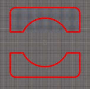
In order to draw the footprint, I will start by creating regions on the top layer in the desired shape. Then a small pad will be placed in the centre of the regions and lastly the desired expansions masks will be set for each of the region.

1. Following the suggested footprint in the datasheet I place an outline using tracks and arcs on the top layer in the PCB Library Editor. The customizable grids are helpful for precisely positioning the outline elements.

2. I create a region from the outline with the menu command Tools > Convert > Create region from selected primitives. Personally, from here I like to move the outline primitives to Mechanical Layer 31, which I consider a construction layer.

3. Then I place 0.5mm pads at the center of the regions. The region drawing mode has been set to draft in the below screenshot so that the pads are easier to see.

4. Next for each of the region that define a pad, I set the Solder Mask Expansion Mode and Paste Mask Expansion Mode to “From Rule”. Once placed on a PcbDoc the solder and mask expansions will be set as determined by the design rules.

5. Finally I add a silkscreen outline.

Now that the footprint for our inductor is drawn, we can continue by creating a schematic symbol that can be used in a design.

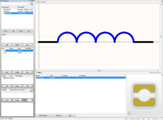
6. In the Schematic Library Editor I create a new component and assign it with the symbol reference of SRR5028. I place two pins with names that correspond to the pad designators I used in the footprint, then link the symbol to the newly created SRR5028 footprint. The model preview window in the bottom right of the screenshot shows the newly created footprint.

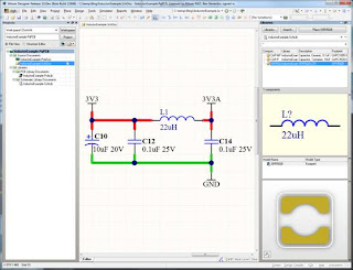
7. Then I create a simple project to which I add the PcbLib and SchLib files I created in the previous steps. The project contains a single Schematic Document with the circuit shown below.

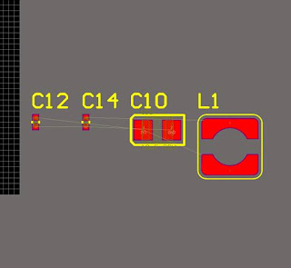
8. I add a new blank PcbDoc to the project which I’ve called InductorExample.PcbDoc. From the PCB editor I run the “Tools->Import Changes From InductorExample.PrjPCB” command to generate an ECO that will add the nets and components to the PCB.

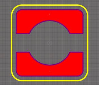
After accepting the ECO changes, the state of the InductorExample.PcbDoc is shown below. The regions that we added to the SRR5028 were treated as an extension to the component pads and consequently the nets that were applied to the pads were also applied to these regions.

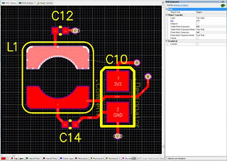
9. I then finish the design by placing the components and adding some routes.

During this editing process, it is important to note that the regions used to define the custom pad shapes continue to be treated by the PCB editor as a separate object.

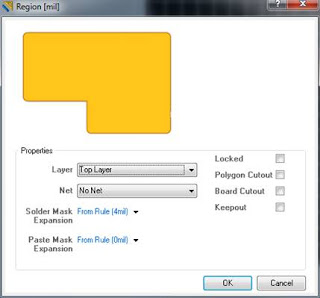
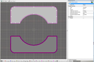
For instance, when the region defining such a custom shaped pad is selected, the inspector shows the properties of a region (and not one of a pad). In this case, it indicates that the Solder Mask expansion of the region in the SRR5028 footprint is 4mil, and is been set by the design rule.

With these enhancements, it should now be much simpler and straightforward to efficiently create and use custom pad shapes.

I’m looking forward to reading your comments and thoughts on the approach we’ve taken, in the comments section below. These have shown to be very insightful and ultimately very useful in helping us provide you with a more streamlined and productive tool.

Thank you very much for your contribution! I am looking forward to reiterate this experience for new projects in the future.


12th update for Altium Designer 10

The Altium Development team are pleased to announce a new update for Altium Designer.

This update includes a new Schematic feature: Specific No ERC Directives. This was introduced in response to BugCrunch report #152 and was further discussed with the Altium Community in the AltiumLive Blogs (read first blog and second blog). The No ERC Directives can now suppress specific violations so that only the selected warning or error conditions are suppressed and any other warning or error will be detected and reported.

Read more about this new feature in the wiki under Schematic No ERC.

This update also includes 14 BugCrunch fixes in addition to the No ERC Directives. These include:

  1. Added the options to include all notes, exclude collapsed notes, or exclude all notes from print and PDF outputs.
  2. The "Update from PCB library" command now shows differences between pad holes.
  3. The board insight display panel now redraws the preview panel to match the primitives as they are added to the panel on hover.
  4. Net on shelved polygon is now correctly updated when updated from Schematic document.
  5. PCB DRC now issues warning if document contains shelved polygons.
  6. A new option was added to NCDrill Settings dialogue that will allow the user to output the EIA Binary Drill file or not. The default for this option is to not generate this NCDrill output type.

For full information on this update, read the release notes.

The delivery of this update affects the following 14 modules:

  1. System Components category: Altium Designer Base, Altium Designer Support, PCB System, PCB Support, Schematic System, Soft Design System, Soft Design Support
  2. FPGA Components category: Instrument - Digital IO
  3. Output Generators category: Output - NC-Drill, Output - ERC, Output - STEP, Printer - Schematic
  4. Importers and Exporters category: Importer - CADSTAR, Importer PADS

Installation of these updated modules will bring their revision up to 10.700.22943. The Platform Build number will also update to 10.700.22943 as the Altium Designer Base module is updated.

To update your Altium Designer 10 installation, ensure you are using a license with valid subscription. Go to the Plug-in page (DXP >> Plug-ins and Updates) and select “Update All”. If you don’t see the update, use the “Refresh” link in top right hand corner of the Plugins page.

Note: If you are using a Private Server license or Standalone license, and you have renewed your subscription since activation, you will be required to reactivate your license to obtain this and future updates.

For those who installed directly from DVD, you can access the updates by changing a setting in preferences: System >> Installation Manager, change the Remote Repository Location to http://installation.altium.com


Thursday, October 6, 2011

STMicroelectronics released to the vault

The Hobart Content Team is very pleased to announce the addition of STMicroelectronics to the Hobart Vault.  In this release we’ve added managed components for microcontrollers in the STM32F, STM32L, STM32W and STM8L families. Also in this release, Sensors & MEMS are added to the vault.

STM32F/L

The STM32 family of 32-bit Flash microcontrollers based on the ARM Cortex-M processor is designed to offer new degrees of freedom to MCU users. It offers a 32-bit product range that combines high performance, real-time capabilities, digital signal processing, and low-power, low-voltage operation, while maintaining full integration and ease of development.

STM32W

STM32W expands the STM32 family to the wireless domain bringing outstanding radio and low-power microcontroller performance. With a configurable total link budget up to 109 dB and the efficiency of the ARM Cortex-M3 core, the STM32W is a perfect fit for the wireless sensor network market. These devices are also IEEE 802.15.4 compliant and support popular protocol stacks such as RF4CE, ZigBee-PRO and 6LoWPAN.

STM8L

The STM8L EnergyLite family are an ultra-low-power MCU based on the 8-bit STM8 core.  Using ST’s proprietary ultra-low leakage process, STM8L features ultra-low power consumption with the lowest power mode of 0.35 µA.

Sensors & MEMS

This initial release covers MEMS-based sensors including accelerometers, gyroscopes, digital compasses, functional sensors including pressure sensors and microphones, and iNEMO inertial modules.

These STMicroelectronics components can be found in the Hobart Vault under

Components\STMicroelectronics

AltiumLive Subscribers can use these components by connecting to the Vault directly from Altium Designer 10 using their AltiumLive credentials, or by browsing to the AltiumLive Design Content area and selecting the Altium Hobart Vault.


Friday, September 23, 2011

Hobart Content Team - Microchip's PIC families (PIC24F, PIC24H & PIC32)

Announcement: Microchip PIC update released to the vault

the release of Microchip’s PIC24E family to the Hobart Vault.  In this release we’ve also made updates and added new components to the PIC24F, PIC24H and PIC32 families.

PIC24E

Microchip’s PIC24E general purpose microcontroller family features the highest speed 60 MIPS core with excellent performance and code density.  It offers superior ADC performance, enhanced CAN communication, easier graphic display interface through 8-bit parallel master port and up to 15 DMA channels for extensive data movement.

Updates to PIC24F/H include the addition of component URLs, pin names in schematic symbols updated to the latest datasheet spec, and 173 new components.

PIC32 has also had pin names updated according to the current datasheet along with another 346 new components.

These Microchip components can be found in the Hobart Vault under Components\Microchip\

AltiumLive Subscribers can use these components by connecting to the Vault directly from Altium Designer 10 using their AltiumLive credentials, or by browsing to the AltiumLive Design Content area and selecting the Altium Hobart Vault.


Monday, September 19, 2011

Hobart Vault Update - Silicon Labs

The Hobart Content Team is very pleased to announce the release of components from Silicon Labs to the Hobart Vault.

 Silicon Labs is an industry leader in the innovation of high-performance, analog-intensive, mixed-signal ICs. The first of several families of components we plan to cover, today we’ve released the following:

MCU Analog-Intensive

This microcontroller family combines the industry’s highest speed 8-bit 8051 MCU core with the highest precision analog peripherals, making them ideal for analog and computation-intensive applications.

MCU Automotive and Industrial

These microcontrollers are auto-grade products qualified and tested to the AEC-Q100 specification with high temperature operation up to 125 °C.  They each include a CAN 2.0B interface, LIN 2.1 interface, an integrated precision oscillator, 1.8 to 5.25 V supply voltage and a 12-bit ADC.

Sensors

The QuickSense Si11xx family is the industry's most sensitive active infrared proximity sensors, enabling innovative touchless human interface applications with ultra-low power advantages.

These Silicon Labs components can be found in the Hobart Vault in Components\Silicon Labs\

AltiumLive Subscribers can use these components by connecting to the Vault directly from Altium Designer 10 using their AltiumLive credentials, or by browsing to the AltiumLive Design Content area and selecting the Altium Hobart Vault.


Wednesday, September 14, 2011

Update 11 for Altium Designer 10 available

This update addresses further issues that have been raised in BugCrunch, including:

  1. Creating a PDF in the OutJob from a 3D Print job no longer keeps the board flipped in the PCB editor
  2. ODB++ output no longer generates incorrect image and EDA package data for offset rounded pads.

Along with these issues, there are also further updates for the PADS and Allegro importers, generating of ODB++, as well as localizations. For detailed information on what is delivered with this update, read the release notes.

The delivery of this update affects the following 9 modules:

  1. System Components category: Altium Designer Base, Altium Designer Localization, Altium Designer Installation System, PCB Support
  2. Output Generators category: Output - AdvPcb3DPrint, Output - ODB, Output - Gerber
  3. Importers and Exporters category: Importer - Allegro, Importer - PADS

Installation of these updated modules will bring their revision up to 10.651.22821. The Platform Build number will also update to 10.651.22821 as the Altium Designer Base module is updated.

To update your Altium Designer 10 installation, go to the Plug-in page (DXP >> Plug-ins and Updates) and select “Update All”. If you don’t see the update, use the “Refresh” link in top right hand corner of the Plugins page.

For those who installed directly from DVD, you can access the updates by changing a setting in preferences: System >> Installation Manager, change the Remote Repository Location to http://installation.altium.com

If you are wanting to install a new build containing this update, please download the latest Installer/Uninstaller to support this build.
 

Creating and importing Step files into Altium for free

This post was brought about by another of our customers needing the ability to create detailed STEP files for their components. Usualy this would entail buying solidworks or something similar.

We knew that we could do it cheAper, and with 3D PCB Design becoming ever more important, we thought we’d share this with the PCB Design community.

Altiums built in 3D extrusion tools are great (and getting better all the time). We expect to see some pretty big jumps in what you can do within Altium in the future. Until that time, try the steps below.

 Step 1

Download and install blender:

Blender

Blender is not a point and click program, so you will need to spend a bit of time getting used to the user interface.  However it is free (open source) and worth the effort of learning, as it’s extremely powerful.

Step 2

Once you have the hang of blender and have created your model (or alternatively you can add one of the standard meshes to try it out).

PCB Layout 3D Model

Now export your model from blender as a .obj or .stl.  We have found .obj gives better results.

PCB Layout 3D Model Export


You now have your model ready for converting to a STEP file.

 Step 3

Download and install STLtoSTEP:

STLtoSTEP

 This programe allows you to convert 3D models from STL (or OBJ) to STEP. This little gem is the key to getting your models into Altium.

Allthough this is a free programe, the developers request that if you use it commercialy then they would appreciate a donation (which is fair).


Step 4

From STLtoSTEP select File>Open OBJ

Browse to and select your recently exported obj model (This may take a while depending on the complexity of your model).

Now select File>Save STEP (FACETS).

Your Step file is now ready to import into Altium.


Step 5

Read your models into Altium.

Your done!


Thursday, September 1, 2011

Hobart Vault Update - Generic SMD Chip Resistors

Today, basic surface mount chip resistors have been released to the Hobart Vault. These cover all E96 resistance values in case sizes from 0201 (0603 Metric) to 2512 (6432 Metric).

A total of over 8,500 resistor parts are now in the vault with supply chain representation from six key manufacturers - Bourns, Panasonic, Rohm, Stackpole, Vishay and Yageo. All part choices for a given design item have been matched according to case size, resistance value, power rating and tolerance.

These first generic components can be found in in the Hobart vault under:

Components - Generic \ Resistors \ Basic Surface Mount.

AltiumLive Subscribers can use these components by connecting to the Vault directly from Altium Designer 10 using their AltiumLive credentials (the best way to see the supply chain information), or by browsing to the AltiumLive Design Content area and selecting the Altium Hobart Vault.


Wednesday, August 17, 2011

Specific NoERC markers - soon to be in Beta

The ‘Specific NoERC markers’ feature was developed over the past couple of months, and it is now about to enter the Beta stage. The feedback provided as comments to the initial blog has been crucial in shaping this new tool into one that hopefully will provide you with more flexibility, accuracy and productivity.

I would like to share with you the near-final shape of this enhancement, so as to gather last minute feedback and ideas, before ‘it goes to press’, so to speak.

In schematic, the specific NoERC markers can now suppress specific error kinds and connection conditions on the net they are  placed on. 

The NoERC marker dialog box now has two pages where such specific errors and conditions can be explicitly ignored, as shown below. These pages are displayed when the ‘Suppress specific violations’ check box is checked

This first screen shot is the page where ERC violations can be chosen to be suppressed.

This is the page where specific connection error conditions can be chosen to be suppressed

The NoERC manager provides a project level view of suppressed errors. It describes the NoERC situation for each net and bus and allows to edit individual NoERC markers from this global viewpoint.

The schematic inspector and list provide a simple way to globally edit sets of NoERC markers in the design. In the first version, we have chosen not to give detailed access of the violation kinds to be ignored from this perspective. This will be the subject of a future improvement.

On screen, the NoERC markers can now be displayed in a variety of shapes, whether they are specific or not.

Combined with colors, this should provide you with a flexible way to give visible meaning to them. At this stage the available shapes are Triangle, Thick cross, Thin Cross, Small cross and Checkbox.

There are several ways a specific NoERC marker can be placed in a design.

A generic NoERC marker can be placed, and then changed to a specific NoERC marker (using the dialog, inspector or the list).

A new placement tool, ‘Place Specific NoERC’ provides you with a way to identify at a glance the nets violating some rules, and to individually place specific NoERC markers for each of the violations..

After compiling, specific NoERC markers can also be placed from the messages panel, by right clicking on a reported violation.

The same can be achieved by right clicking on a schematic object involved in a violation.

The suppressed errors can still be reported by the compiler, if a project option (report suppressed errors) is turned on. In this case they are reported as shown below.

Suppressed errors can also be reported in the ERC output, defined in an output job document (this setting is local to the outputjob document and independant from the project setting). They appear then in the generated report.

Finally, NoERC markers can be excluded from printouts, by shape

This constitutes the extent of the improvements that are about to be released to beta.

As always, your thoughts and feedback are very much welcome, and I will be very interested to read them in the comments section below.

But as this particular project draws to a close, I would like to highlight the importance of your involvement in its definition and completion.

A significant number of elements of this enhancement have been directly influenced by the feedback you have provided.

On a personal level, this provides me with a great deal of satisfaction. Working directly with the people who will ultimately use this feature makes the process a real pleasure. But most importantly, I hope this will constitute a fundamental part of the success of the feature, and really help you to perform your daily work better.


Thursday, August 11, 2011

altium-designer-addons

http://code.google.com/p/altium-designer-addons/

This project contains set of scripts, examples and other content which is developed to provide extended features for Altium Designer unified design environment for electronics development

  •  
  • Custom Pick&Place report script - script for generating user defined P&P for SMD components only
  • SelectConnectedTrack script - script for selection of connected NoNet track on Mech layers
  • CopyAngleToComponent script - script for copying angle of track to a component
  • EagleToAD conversion package - package of scripts for conversion of PCB project from Cadsoft Eagle to Altium Designer (manual available only in Czech)
  • IBIS Editor script - Script that overrides Selector and Submodel keywords in IBIS File.
  • IncrementingDesignators script - Script that enables user to set designators with mouse. Works on Components (in SchDoc and PCBDoc), pins (SCHLIB) and pads (PCBLIB). Designators can be swapped too. When working with pins it can also move pin names.
  • SCH-SelectTouchingRectangle script - Script made because some people wanted select touching rectangle feature in Sch.
  • SCHSelectionFilter script - Script that uses select Touching trectangle, but user can choose object types that will be selected.
  • ZoomComponent script - PCB function similar to Altium's Jump Component, but it also zoom, mask and/or select component.
  • Adjust Component script - it will center the designator in top and bottom overlay.
  • RoomFromPoly script - Script to create room from selected objects or from selected polygon.
  • RenumberPads script - Script helps with changing order of pads mainly in Altium PCBLIBs. You just start script, select start index and increment and you create new designators of pads by clicking on them in the new order.
  • Hyperlynx Exporter script - Script for PCB export to hyp file. It adds fills, regions, polygons and split planes in hyp file.
  • Current Calculator script - PCB script that gives the user a dialog box with current (Amperes) handling calculations for a selected track. The script determines if the track is on an internal or external layer, and provides current calculations for 1, 5, and 10°C rise above ambient.
  • FormatPaintBrush script - This script is used to copy formattings from one object to the others. Currently it works on dimensions and coordinate in PCB and wire in sch. It is planned to be expanded to other objects.
  • DeleteAllSelectedItemsInPCBLIB script - This script can be used to delete selected objects in PCB Library. Currently you can only delete selected objects that are part of currently visible footprint, but this script deletes selected objects that are in other footprints.


Monday, August 8, 2011

Hobart Vault Update - Würth Elektronik

The Hobart Content Team is pleased to announce the release of Würth Elektronik’s SMD Power Chokes and Double Chokes. This is the fourth and final release of Würth components.  Eight categories have now been released over the last two months; an additional 1600 components available in the vault, all with detailed 3D support.

SMD Power Choke

The SMD power chokes of Würth are divided between magnetically shielded and unshielded inductors. The magnetically shielded inductors are represented by the families WE-PD, WE-PD3, WE-PDF, WE-TPC, and the power multilayer inductors WE-PMI. The families WE-PD2, WE-PD4, WE-GF and WE-LQ are magnetically unshielded.

The inductors are optimized for use in switching regulators and DC-DC converters, optimised in the selection of the core and winding design. Furthermore, these components realise a stable inductance over a wide range of frequencies. In the area of switching regulator applications, the choke is used for intermediate storage of electrical energy and also for smoothing the output current.

Nickel-Tin alloy used for the core results in very low losses and high modulations.  This makes them particularly suitable for use in switching regulator applications up to 10 MHz while they offer a high current capacity and low DC resistance in a very small package. The miniature power chokes WE-TPC are suitable for applications where a high package density and a low height are required.

Double Choke

The magnetically shielded WE-DD series of double chokes, in contrast to the single-wound inductors, have two identical, separate windings on a common ferrite core. The application spectrum of this reactor is large, it can be used in 1:1-flyback applications, buck, boost, SEPIC and CUK switching regulators and switching regulators with a second, unregulated output voltage. When using them in series and parallel arrangements, even more choke solutions become available.

All components are available from Würth Elektronik ex stock. Samples are available free of charge. More info at www.we-online.de.


Thursday, July 28, 2011

Update 10 for Altium Designer 10 available

The Altium Development team are pleased to announce a new update for Altium Designer.

This update focuses on addressing further issues that have been raised in BugCrunch, including:

  1. Feature request to reset component designators when copying and pasting in schematic
  2. Angular dimensions will now be correctly saved, no matter how the inside/outside reference points are selected
  3. Implemented “Select touching area” and “Select touching line” for object selection in schematic sheets, libraries and OpenBus documents.

Along with these issues, there are also a few issues fixed for CAMtastic. For detailed information on what is delivered with this update, read the release notes.

The delivery of this update affects the following 3 modules in the System Components category:

  1. PCB System
  2. PCB Support
  3. Schematic System

Installation of these updated modules will bring their revision up to 10.600.22648. The Platform Build number will remain at 10.589.22577 as the Altium Designer Base module is not updated.

To update your Altium Designer 10 installation, go to the Plug-in page (DXP >> Plug-ins and Updates) and select “Update All”. If you don’t see the update, use the “Refresh” link in top right hand corner of the Plugins page.

For those who installed directly from DVD, you can access the updates by changing a setting in preferences: System >> Installation Manager, change the Remote Repository Location to http://installation.altium.com


Tuesday, July 26, 2011

Shanghai Vault Update - VITA CMC Mating Connectors

The Shanghai Content Center is very pleased to announce an update to the previous VITA family release. This week, more mating connectors for the existing VITA Mezzanine standard modules have been added.

These follow the same style as previous mating connector projects, that is complete with signal assignments, connector 3D models and example layouts. These design templates can be used in conjunction with our existing VITA module templates to build up carrier modules.

This release includes mating connectors for FMC, PMC and XMC, and can be found in the VITA - CMC folder of the Shanghai Vault.

FMC and XMC are both provided in single and double variants.

Those on the AltiumLive Subscriber Plan can use these templates by connecting to the Shanghai Vault directly from Altium Designer 10 using their AltiumLive credentials, or by browsing to the AltiumLive Design Content area and selecting the Altium Shanghai Vault


Monday, July 25, 2011

How to import Eagle files into Altium Designer?

There has been some discussion around importing files from Eagle and we have
collected some information which I felt was worth sharing with you. As you are
aware Altium Designer does not currently offer an Eagle importer however there
is a way to import your Eagle Schematic and PCB's into AD. CadSoft, Eagle offers ULP
script's (User Language Program) that will export to an earlier Protel format
which can then be opened in Altium Designer. These scripts use the file
extension [*.ulp].

Using the Eagle export script Tool, it is possible to export Protel ASCII data
from Eagle Schematics and/or PCBs. The resulting ASCII data can be opened with Altium Designer.  Important
Note:
this export tool is not an Altium product, and is not supported by Altium. These below scripts are popular but
there are others floating around as well.

Convert Eagle Schematics to Altium
eagle2ad_sch.ulp

Convert Eagle PCB's to Altium
export-protelpcb.ulp


The information below is mostly for things to be cautious of after a PCB is
converted, others may have more insight as to what to look for after converting
a schematic using the mentioned ulp. The original
scripts can be found at (ftp://ftp.cadsoft.de/eagle/userfiles/ulp/export-protelpcb.ulp), Or (http://www.cadsoftusa.com/downloads/user-language-programs/).

Note: The script can fail if there is a % character (see issue 8).

These ULP's can be helpful however some clean up should be expected. To date
the following issues have become known regarding the PCB export ULP.

1. There is no Board Header Record
2. The Layer designators in the inner layers are not correctly shown. It is possible to search for these incorrectly shown Layer designators with a text editor (e.g., Notepad) and to replace/rename these discrepancies. (e.g.
Routex –> Midx) Midx is the designator recognized by Altium Designer
3. After the PCB Import, design rules must be made and checked.
4. Plane layers may be omitted. These are however easy to create in Altium Designer as long as there no Split Planes were present.
5. There are cases where Overlay-Objects from components end up on the wrong layers. You can unlock and select the component
primitives, and then change layers for any discrepancies.
6. All pads come in a Pad Designator 1. This will have to be corrected if this is ever to map to schematic symbols. However, all primitives for a
component are at least grouped into a component.
7. All the tracks came in but were not assigned to any nets. They were all No Net.
8. The script chokes if a percent sign (%) is included in any text (such as a Comment with "1000uF 5%"). This is because the
script sends this to Printf() as a format string, which interprets it as the
start of a new field for which there is no corresponding parameter passed.

Steps in Eagle
1. Open Eagle
2. Go to File / Open / "Browse to Eagle PCB" or Eagle "Schematic"
3. Go to File / Run / "Browse to the ULP you want to run. (ie: schematic or pcb export ulp

Hope this information is helpful...